 |
||||||||||||||
The aim of this department is to develop the environmentally conscious smart green technology and its theoretical basis which contributes the reduction of the environmental impact in manufacturing, waste treatment and recycle processing. Especially, the research focused on the following topic are main targets; substitution of materials to toxic free and ecomaterials in electronics assembly, the use of low environmental impact materials in joining process, enhancement of reliability of fine-pitch high density packaging, establishment of design for reuse, evaluation method of reliability for reuse of components, and development of sorting technology for high quality recycle of materials. Furthermore, the department aims to develop the high reliability joining technology for manufacturing of new equipments for effective use of energy. |
 |
 |
 |
|||||||||||
| Assoc.Prof. H. Nishikawa |
S.A.Researcher O. Mokhtari |
S.A.Researcher M.-H. Roh |
||||||||||||
|
||||||||||||||
 |
||||||||||||||
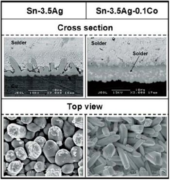
Control of microstructure between lead-free solder and base metal: The microstructure after lead-free soldering closely relates the reliability of joints, therefore, the control of interfacial structure is quite important to enhance the life of electronics. Figure shows the intermetallic compound formed between lead-free solder and copper base metal. |
||||||||||||||
.jpg) |
.jpg) |
|||||||||||||
High performance of conductive adhesive bonding: To improve the performance of conductive adhesive, the investigation into the effect of the addition of various particles into conductive adhesive on the electrical property of conductive adhesive has been performed. (a) SEM micrograph of cross section for conductive adhesive with low melting point metal.
|
||||||||||||||
 |
||||||||||||||
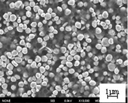
Isotropic conductive adhesives (ICAs) using copper filler: Instead of silver filler, in order to apply copper filler to ICAs, surface-modified copper fillers such as silver-coated copper filler and copper filler protected organic layer have been investigated. Figure shows the appearance of copper filler with organic layer in resin after curing at 175 ℃ for 1 h. |
||||||||||||||