Research Areas
Research Division of Materials Joining Process
Dept. of Energy Control of Processing
The main research subject is the development of the high density energy source for processing advanced materials having special functions and properties. We undertake fundamental investigations of the characteristics of the high energy source interacting with materials, and we study advanced control techniques for optimizing the energy transport.
Major emphasis is placed on the generation, control and energy/mass transfer in arc plasmas, which are a high density energy source that have been applied to a variety of materials processing techniques such as weld-ing, cutting, heating, high temperature processing, surface modification, additive manufacturing and the synthesis of ultrafine powders.
1. Generation and control of thermal plasmas, and their application to welding and joining processes
2. Arc physics, molten pool behavior, and transport theory in fusion welding
3. Development of new arc electrodes based on the analysis of electrode-plasma interaction
4. Development of environment-friendly smart arc welding processes
5. Development of new generation material processes using atmospheric pressure plasma
6. Control of arc discharge in lighting and electrical devices
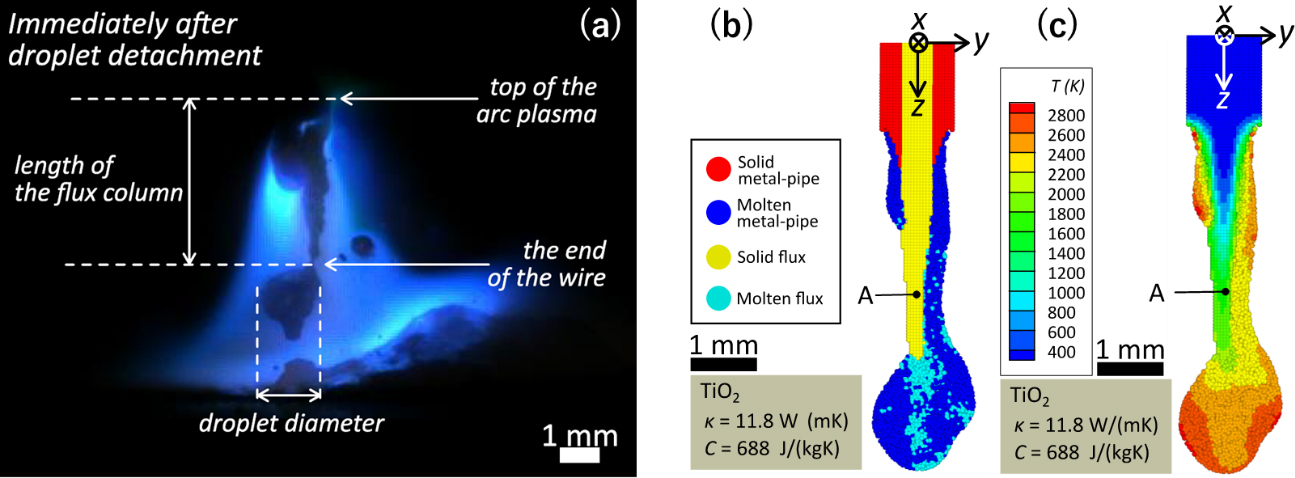
(a) Dynamic 3D imaging spectroscopy system and (b) the resulting non-axisymmetric dis-tributions of electron number density (top) and electrical conductivity (bottom) in a MIG arc. The regions indicated by a dashed line correspond to areas where the measurement accuracy is reduced due to the presence of the droplet and the wire. When a cathode spot appeared at the location marked by the red circle, the electrical conductivity and electron number density within the region enclosed by the solid black line became higher than before the spot formation. Once the cathode spot disappeared, both the electrical conduc-tivity and electron number density decreased. Such localized increases in electrical con-ductivity and electron number density suggested that the welding current was concentrated at the cathode spot. As a result, a biased electromagnetic force acted on the molten wire, causing the droplet to be transported in the direction opposite to the current concentration, as revealed by this measurement.
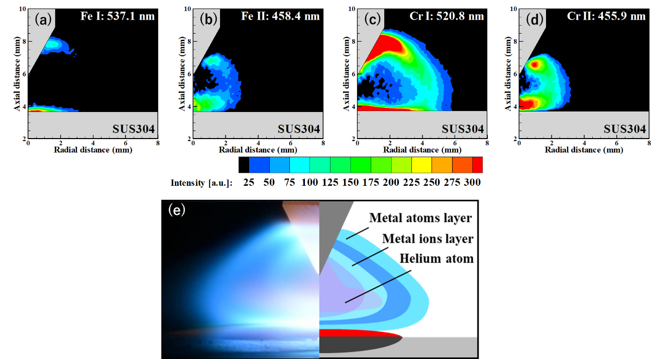
Time histories of welding current and tungsten electrode tip temperature during AC TIG weld-ing (upper left), and temperature distributions at representative times (bottom). The electrode temperature increased during the EP period primarily due to heating by electron infl ow, where-as it decreased during the EN period as a result of cooling by thermionic emission. At 3.5 ms, corresponding to the latter half of the EP period, a molten metal droplet was ejected from the high-temperature region at the electrode tip. The upper-right fi gure also shows the superimposed trajectories of ejected droplets, where larger values indicate a higher frequency of droplet pas-sage. This study revealed that the droplet ejection originates from gasifi cation occurring within the molten high-temperature region at the electrode tip.
Members
Prof.
M. TANAKA
Assoc. Prof.
H. KOMEN
Assist. Prof.
S. TASHIRO
Research Division of Materials Joining Process
Dept. of Energy Transfer Dynamics
Our research activities encompass works on development of process control technologies of surface and interface for advancement of materials joining science and processing technologies through creation of novel process-energy sources (plasmas and particle beams), and span the range of applications from functionalization of materials to their process control. These research activities are based on fundamental studies on energy transfer dynamics involved in a variety of materials processing with process-energy sources.
Specific areas of research include low-temperature formation of high-qualitythin-film transistors and large-area low-damage processes. Furthermore,based on studies on spatio-temporal control of discharge for innovative plasma medicine, advanced processes have been developed for joining of dissimilar materials, mist CVD and green technology including methanation.
1. Studies on plasma-materials interactions for development of advanced process technologies
2. Development of novel plasma sources and particle beams for advanced process technologies (CVD, PVD)
3. Development of novel large-area, low-damage and high-density plasma sources for advanced process control of functional materials
4. Creation of softmaterial processing science for development of advanced green nanotechnologies with inorganic/organic flexible hybrid structure
5. Studies on temporal and spatial control of discharge for development of innovative plasma sources for plasma medicine
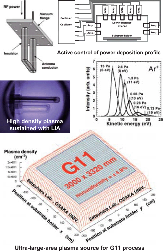
Low-damage and ultra-large-area plasma source with multiple low-inductance antenna modules
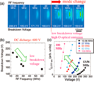
Development of innovative plasma source for plasma medicine
(a) ICCD images of atmospheric RF plasmas
(b) Frequency dependence of discharge breakdown voltage
(c) Frequency dependence of O optical emission intensity
Members

Prof.
Y. SETSUHARA

Assoc. Prof.
K. TAKENAKA

Assist. Prof.
S. TOKO
Research Division of Materials Joining Process
Dept. of Micro Joining
The main research objectives are for electronics packaging to develop advanced joint materials, to establish advanced micro joining processes, and to elucidate the mechanisms of the micro joining processes. Especially, the creation of the functional joint materials, the development of novel advanced micro processes by various energy sources, the understanding of interfacial behaviors in nano-/micro-scale, and the enhancement of the highly reliable joints based on the control of interfacial structure and performance are performed.
1. Development and evaluation of advanced micro joining process
2. Elucidation of micro joining phenomena and defect suppression
3. Control and analysis of microstructure at soldered interface
4. Development of low-temperature solder alloys contributing to the reduction of CO2 emissions
5. Formation of high heat-resistance joint using three-dimensional nanostructure
6. Elucidation of interfacial bonding mechanisms through atomistic simulation
7. Macro-micro simulation for joint-property prediction
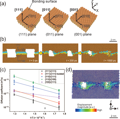
Molecular Dynamics (MD) simulation results on Cu-Cu bonding behavior:
(a) Bonding interfaces replicating various crystal orientations,
(b) Void closure behavior at the interface,
(c) Diffusion coefficients on the bonding interface with various orientations,
(d) Atomic displacement vectors analysis.
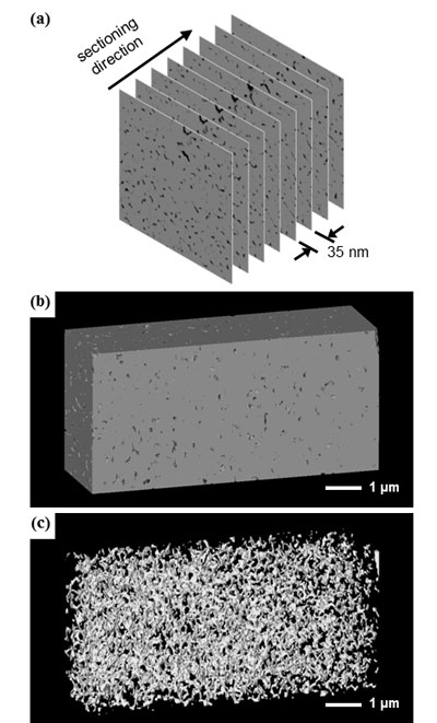
Microstructure of sintered joint using Ag nanoparticle paste
(a) Serial sectioning of Ag sintered layer by FIB/SEM system
(b) Reconstructed 3D image of Ag sintered layer
(c) Reconstructed 3D pore distribution into Ag sintered layer
Members
Prof.
H. NISHIKAWA
Assoc. Prof.
H. TATSUMI

Assist. Prof.
M. IIOKA
Research Division of Materials Joining Process
Dept. of Laser Materials Processing
Fundamental studies are performed concerning joining, cutting, surface modification and removal processing with laser beams, aimed at advanced fusion between laser science and production engineering. We focus on clarification of welding or joining mechanisms and intelligent monitoring technology on the basis of the visualization of material processing phenomena with high-speed optical observation or X-ray transmission imaging techniques. Moreover, laser should be utilized with not only high thermal efficiency but also physicochemical effects induced by interaction between light and material. Thus we create innovative processes including laser direct joining of metal and plastic, put these processes to practical use and disseminate achievements of our research to the world.
1. Development and evaluation of joining and welding processes for the advanced functional materials.
2. Elucidation of laser welding phenomena and imperfection formation mechanisms and development of remedies.
3. Fundamental studies on laser interaction with materials and fundamental studies of materials processing utilizing laser.
4. Creation of new function by surface modification with laser.
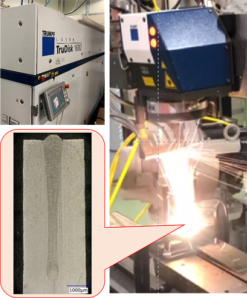
Clarification of laser welding phenomena
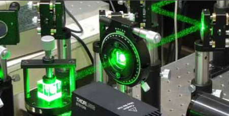
Clarification of laser materials interaction
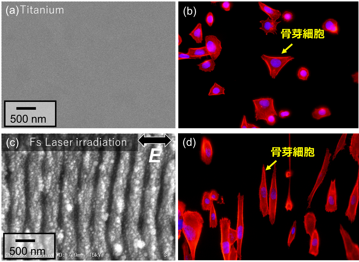
Development of Laser induced surface modification technology for adding of new functions,
(a)bare Ti,
(b)Cell on bare Ti,
(c)periodic nano-structure on Ti surface formed with femtosecond laser system
(d)Cell on periodic nano-structure
Members
Prof.
M. TSUKAMOTO

Assoc. Prof.
Y. SATO

Assit. Prof.
K. TAKENAKA

S.A. Prof.
S. KATO

S.A. Researcher
J. TOKUMOTO
S.A. Researcher
E. HORI

S.A. Researcher
A. Yonezawa
S.A. Researcher
N. YOSHIDA
S.A. Researcher
N. Asahi
Research Overview
Research Division of Materials Joining Process
Research Division of Materials Joining Mechanism
Research Division of Materials Joining Assessment
Research Center for Additive Joining Application (RAJA)
Strategy Office for Promotion of Inter-Institute Collaborations
Joint Interface Microstructure Characterization Room
Global D&I Promotion Office
New Normal Manufacturing Consortium Office
Research Alliance Laboratories
Joint Research Chair
International and Industry-academia Joint Research Center